Semiconductors: A Microcosmic Manufacturing Marvel

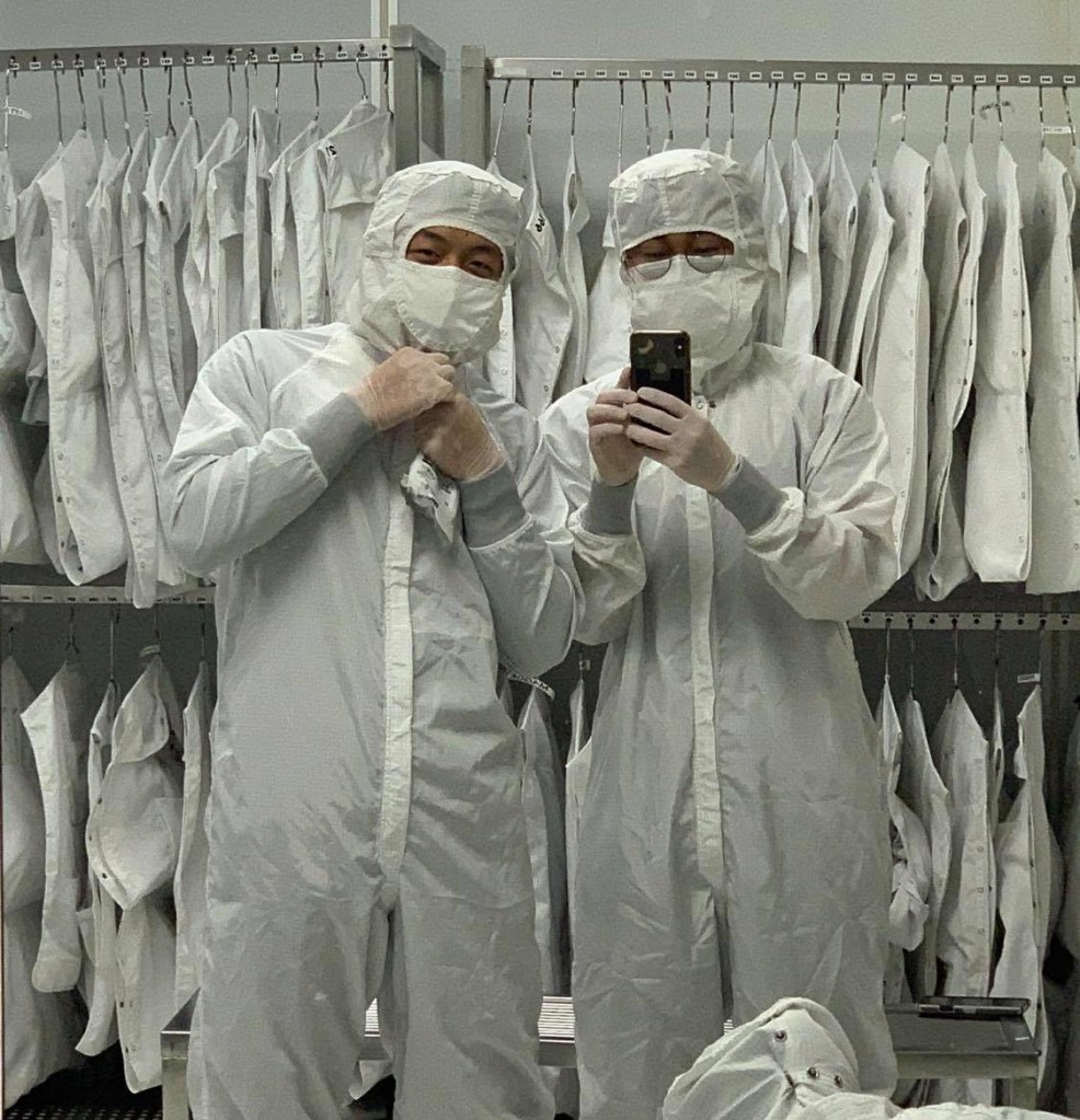
Over the summer of 2021, I was blessed with the opportunity to intern in-person with Formfactor Inc., the leading provider of semiconductor metrology equipment and a cornerstone to the semiconductor supply chain. At Formfactor, my work revolved around internal quality assessment which provided me with hours of Python and AutoCAD experience along with a bit of JMP and Matlab sprinkled in. I worked heavily with optical measurement equipment which provided me with the data necessary for error analysis. However, I won’t bore you with further details regarding my day-to-day tasks. The NDA I signed upon exiting may or may not play a part in my silence as well. This internship was my first real exposure to the semiconductor industry and micron/nanoscale technology. To say I am impressed by the inexplicably complex processes that comprise of the semiconductor supply chain is an understatement. The crazy levels of ingenuity that go into the hardware that allows everyone from software engineers to write “print(‘hello world’)” to the Gen Zer to scroll through TikTok are simply ignored and underappreciated. So, with this time, I would like to enlighten everybody who many not already know about how the beautiful chips that form the basis of all technology surrounding you come to be.
Let’s start from the ground-up, literally
Semiconductors start with silicon, a material abundant in the earth’s crust that also exhibits a desirable set of conductive properties. Silicon is mined in raw form and purified. Afterwards, the semimetal is melted down in a vat. In its molten form, a seed crystal is inserted into the liquid and spun. Slowly and while spinning, the crystal is withdrawn from the vat vertically. Silicon solidifies along this seed crystal until a consistent diameter of material solidifies. Once the seed crystal has been fully withdrawn, the silicon resembles a cylinder with a rough surface and pointed edges. The pointed edges are removed and the rough surface is smoothened by lathe until we are left with a near-perfectly cylindrical piece of stock silicon material. This material is cut into thin slices of circular pieces of silicon which are called silicon “wafers”. Leading blank wafer producers include Hemlock and Okmetic. Never heard of them right? That’s because the high-profile companies are further down the process. With this slab of silicon mined and primed, the engineers go to work.
Electrical Engineers, have at it

When it comes to designing the actual circuits that are contained within chips, electrical engineers have all the fun. Here, schematics are drawn which serve as the blueprint for the manufacturing process. These designs are unique and specific to the purpose that the chip will serve. In layman’s terms, the electrical engineers determine “what needs to created”, while the rest of us are concerned with “how to create it”. Commonly, these designs are created by some individual device makers such as Intel and Texas Instruments or by fabless companies such as Qualcomm. IDMs have typically vertically integrated their operations and are responsible for both designing AND manufacturing their own chips. Fabless companies on the other hand are only concerned with circuit design and sell their designs to Foundries, which exclusively manufacture the design.
Baton handoff to the Chemical Engineers

Once the electrical engineers have had all the fun exercising their creative liberty without much concern for feasibility, the chemical engineers begin thinking about how the heck such an expansive circuit network on paper will condense to a chip no more than the size of your pinky fingernail. Chemical Engineers might as well be called Disney Imagineers because this is where the magic happens. Using processes such as photolithography, chemical dry/wet etching, and/or laser cutting, chemical engineers create layers upon layers of 2-D profiles on the wafers which come together to form the aforementioned 3-D chip. Each wafer is etched with hundreds of chips with identical circuitry. This process is commonly simplified to “fabrication” and is indisputably the most complex and disruptive manufacturing technique to date. The concept of Moore’s Law (the trend that our chips and thus our devices are exponentially decreasing in size) is powered by the ingenuity of newer and more efficient fabrication techniques. Fabrication is powered by both the aforementioned IDMs as well as foundries which exclusively fabricate and do not design the circuit schematic. These foundries include some well-known companies such as Samsung and TSMC.
Mechanical Engineers, time to shine

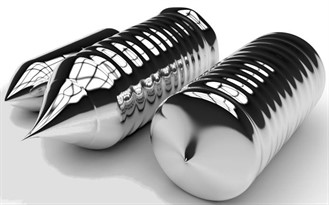
For the final leg of the semiconductor race, I would like to tie the process back to my people: the Mechanical Engineers at Formfactor. We design the systems and tools which others use to perform quality screening on their etched wafers. Each wafer containing hundreds of chips will need to have electrical signals sent through each chip. Ideally the proper output reading should be measured off of a good wafer. Mechanical Engineers design the electrically, structurally, thermally, and dimensionally robust probe heads that make hundreds of thousands of contacts with the wafer at once. Individual contacts are made by tiny metal springs less than 1/10th the girth of a human hair. This is clearly much more efficient than having an operator manually traverse across the wafer tp make contact with tiny touchpoints using a multimeter. Lastly, after a wafer has been deemed “good” based on the readings taken from our probe heads, the wafer is sent to be laser cut into individual units, which are subsequently packaged up into that familiar black casing that encloses all chips.
The Quantum Dark Horse
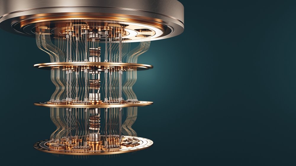
I would be remiss if I were to talk so much about traditional semiconductors without mentioning my curiosity with the rapidly developing rookie in the computing race: quantum computing. Quantum computing is expected to be present in our daily lives within 5 years from now. The beauty of quantum computing lies in turning the discrete into the continuous. Traditional semiconductors create logical bits that must only be 1 or 0, indicating only the presence or absence of the proper electrical signal. Quantum computing turns towards the position of a subatomic particle and produces a q-bit, which may be 1, 0, or some combination of both. Many companies have long noticed this trend and have moved to acquire equipment capable of making quantum calculations and measurements. Often, these pieces of equipment face the challenge of maintaining an extremely cold environment in an attempt to mitigate any quantum noise and slow the motion of subatomic particles down to a measurable level. However, quantum computing is not the end-all-be-all. There are certain applications which traditional computing is simply better suited for. So calm down Apple, your iPhone is not irrelevant… yet.
I hope you learned something from my blurb about the fundamentals of computing. I know all too many people who express a desire to be able to connect what seems to be their completely separate digital world with the physical world, and I hope my post has helped shed some light on that. Altogether, I want to send a huge “thank you” over to the wonderful engineers at Formfactor for taking me in over this pandemic summer. I’ve learned a lot about what I don’t yet know, and that is a priceless gift.